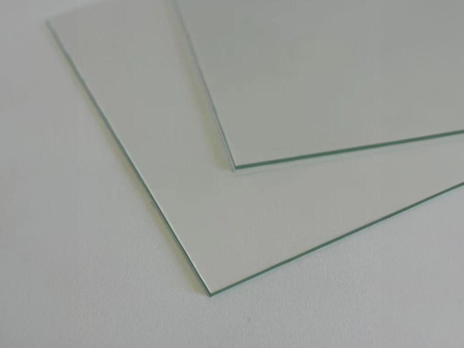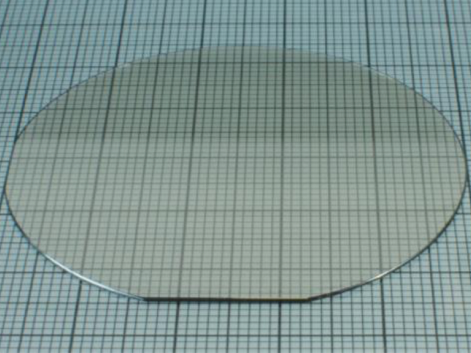
NANOSSR offers premium quality GaN crystal substrates with low dislocation density (on the order of 105 /cm2) and uniform surface with no periodic defects. These high quality GaN crystals have an usable area of more than 90%.
We offer the best price on the market for high quality GaN crystal substrates. Customers from all over the world have trusted NANOSSR as their preferred supplier of GaN crystal substrates.
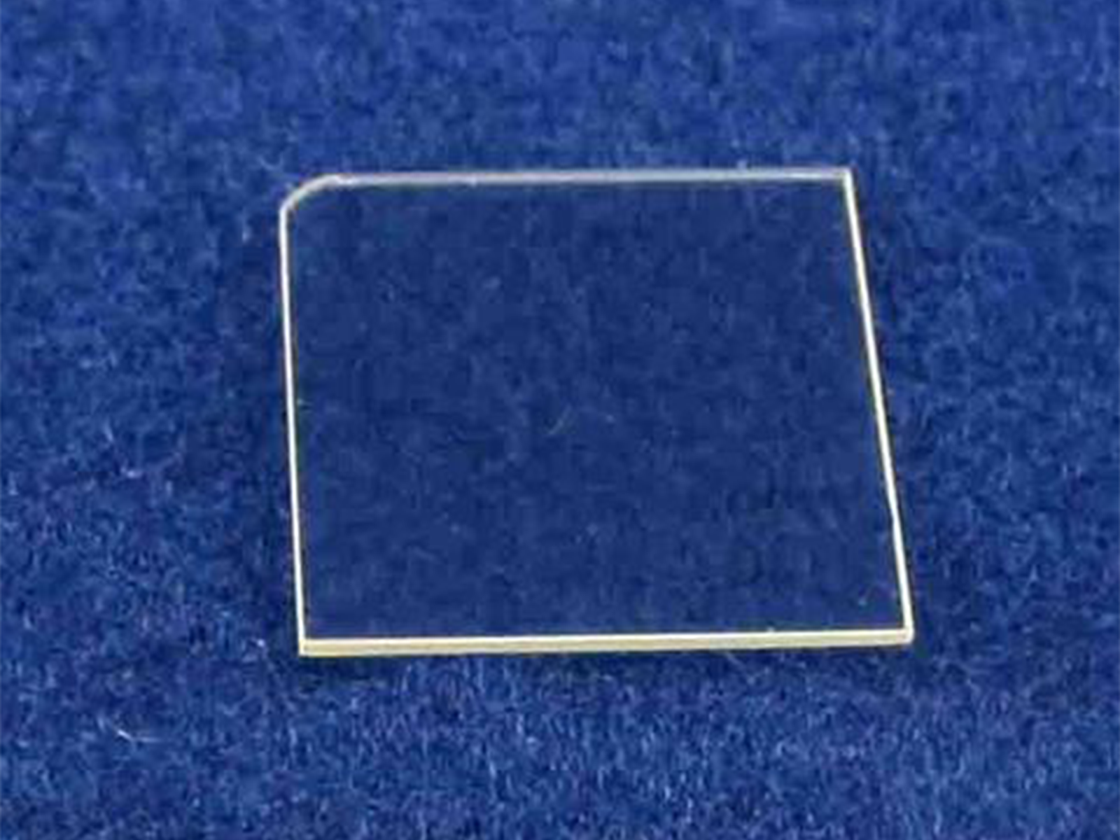
Product #: WA0225
- Conductivity type: semi-insulating
- Dimension: 5 mm x 10 mm +/- 0.2 mm
- Thickness: 350 +/- 25 um
- Usable surface area: > 90% substrate surface
- Orientation: M plane (1-100)
- Total Thickness Variation:
- Bow:
- Resistivity (300K): > 106 Ohm-cm
- Fe-doping concentration: ~ 3 × 1018 cm−3
-
Dislocation Density: 5 cm-2
- Polishing: front surface Ra
- Package: packaged in a class 100 clean room environment in single wafer containers under a nitrogen atmosphere.
Related References
GaN grown in polar and non-polar directions
http://www.wat.edu.pl/review/optor/12(4)339.PDF
In this paper, defects formed in GaN grown by different methods are reviewed. Thin GaN films were grown on c-, m-, and a-planes on a number of substrates and typical defects as characterized by transmission electron microscopy are described. For polar epilayers grown on c-plane sapphire the typical defects are dislocations (edge, screw and mixed). The lowest dislocation density was obtained for homoepitaxial growth using molecular beam epitaxy (MBE) or hydride vapour phase epitaxy (HVPE). In these cases, the core structure of screw dislocations were studied in detail. In both cases, the cores are full. In the layers grown by HVPE the dislocations are decorated by pinholes stacked on top of each other. These pinholes are empty inside and their formation is attributed to impurities (oxygen) present in these layers. In these layers Ga-rich cores have been found. These were not observed in the layers grown by MBE on the top of the HVPE templates. Epilayers grown in non-polar directions (m- or a-plane) have a high density of planar defects (stacking faults) terminated by partial dislocations. Only low energy faults were found. The majority of these faults are formed at the interface with the substrate and propagate to the sample surface.